| CPC H01L 27/1464 (2013.01) [H01L 27/14618 (2013.01); H01L 27/14625 (2013.01); H01L 27/14636 (2013.01); H01L 27/14687 (2013.01); H01L 2924/0002 (2013.01)] | 20 Claims |
|
1. A device comprising:
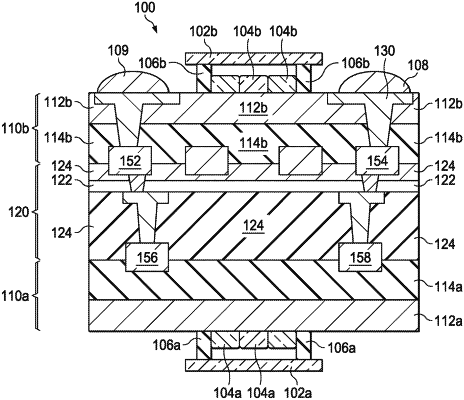
a first image sensor element having a first surface that includes a first conductive portion and a first dielectric portion;
a second image sensor element having a photosensitive region and a second surface that includes a second dielectric portion;
a processing element disposed between the first and second image sensors, the processing element having a third surface that includes a second conductive portion and a third dielectric portion and a fourth surface that include a fourth dielectric portion, wherein the second conductive portion directly interfaces with the first conductive portion, the third dielectric portion directly interfaces with first dielectric portion and the fourth dielectric portion directly interfaces with the second dielectric portion; and
a first conductive feature extending from the photosensitive region to the processing element.
|