| CPC H01L 27/14636 (2013.01) [H01L 24/16 (2013.01); H01L 27/14618 (2013.01); H04N 23/54 (2023.01); H01L 2224/16227 (2013.01)] | 13 Claims |
|
1. An imaging apparatus comprising:
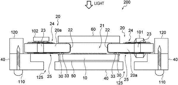
a sensor chip;
a wiring board having a glass base material and a laminated wiring layer; and
a protective member that protects the sensor chip, wherein:
the sensor chip and the wiring board are joined via a bump unit including a plurality of bumps,
the bump unit includes a first bump and a second bump,
the first bump is formed on the sensor chip and the second bump is formed on the first bump before the sensor chip and the wiring board are joined,
each of the plurality of bumps is formed by conductive members having substantially same composition, wherein
an adhesive is arranged on the glass base material and the laminated wiring layer of the wiring board, and the glass base material and the laminated wiring layer of the wiring board are adhered to the protective member, and wherein
the adhesive includes a first adhesive and a second adhesive such that the first adhesive is arranged on a side surface of the glass base material and is arranged up to the protective member, and
the second adhesive is arranged between the glass base material and the protective member.
|