| CPC H01L 27/1463 (2013.01) [H01L 27/14621 (2013.01); H01L 27/14623 (2013.01); H01L 27/14627 (2013.01); H01L 27/14629 (2013.01); H01L 27/14636 (2013.01); H01L 27/14645 (2013.01); H01L 27/14656 (2013.01)] | 15 Claims |
|
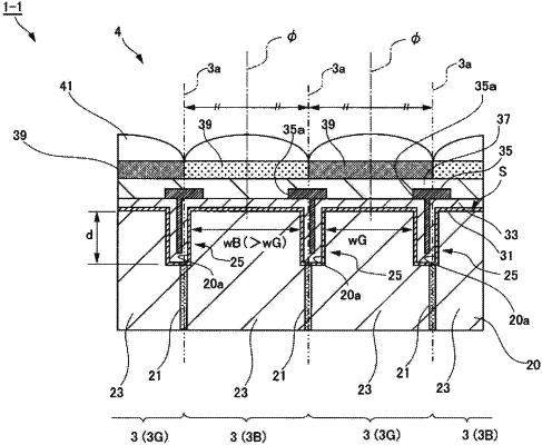
1. A light-detecting device, comprising:
a semiconductor substrate having a first side as a light incident side and a second side opposite to the first side, the first side and the second side each extending in a first direction;
a plurality of photoelectric conversion units disposed in the semiconductor substrate;
a first trench region disposed in the semiconductor substrate between two of the plurality of photoelectric conversion units in the first direction;
a first light shielding region disposed above the first side, wherein the first light shielding region is above at least a part of the first trench region in a second direction, the second direction being perpendicular to the first direction, and the first light shielding region is offset from a center portion of the first trench region in a third direction;
a second trench region disposed in the semiconductor substrate adjacent to at least one of the plurality of photoelectric conversion units in the first direction; and
a second light shielding region disposed above the first side, wherein the second light shielding region is above at least a part of the second trench region in the second direction and offset from a center portion of the second trench region in a fourth direction opposite the third direction,
wherein a distance between a center of the first trench region and a center of the second trench region is different from a distance between a center of the first light shielding region and a center of the second light shielding region in a cross-sectional view.
|