| CPC H01L 27/14623 (2013.01) [H01L 27/14618 (2013.01); H01L 27/14636 (2013.01); H01L 27/14685 (2013.01)] | 19 Claims |
|
1. An image sensor package comprising:
a package substrate;
an image sensor chip on the package substrate;
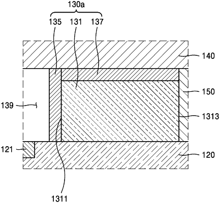
a dam structure on the image sensor chip and comprising a dam main body having an opening and a first light absorption layer on an inner wall of the dam main body;
a transparent substrate on the dam structure; and
an encapsulant contacting the image sensor chip and an outer wall of the dam main body,
wherein the dam structure further comprises a second light absorption layer on an upper surface of the dam main body, and
wherein the second light absorption layer vertically overlaps the whole dam main body.
|