| CPC H01L 27/14621 (2013.01) [H01L 27/1463 (2013.01); H01L 27/14603 (2013.01); H01L 27/14645 (2013.01)] | 20 Claims |

|
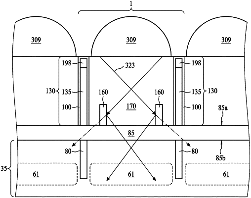
1. A method for fabricating an optical structure, comprising:
forming a light detection region in a substrate;
forming an isolation structure at least surrounding the light detection region; and
forming a primary grid over the isolation structure, comprising:
forming a metal layer over the isolation structure;
forming a first dielectric layer over the metal layer; and
partially removing the metal layer and the first dielectric layer with a first mask by patterning;
forming a secondary grid at least partially surrounded by the primary grid laterally; and
forming a liner lining at a sidewall of the primary grid, wherein the liner is free from being in direct contact with the secondary grid.
|