| CPC H01L 27/14618 (2013.01) [C08K 3/22 (2013.01); C08K 3/36 (2013.01); H01L 27/1463 (2013.01); H01L 27/1464 (2013.01); H01L 27/14627 (2013.01); H01L 27/14636 (2013.01); H01L 27/14683 (2013.01); C08K 2003/2227 (2013.01)] | 19 Claims |
|
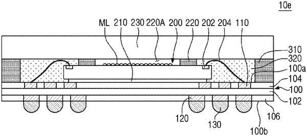
1. A semiconductor package comprising:
a package substrate;
a semiconductor chip mounted on the package substrate;
a transparent substrate disposed on the semiconductor chip;
an attachment dam between the semiconductor chip and the transparent substrate, the attachment dam extending along an edge of the semiconductor chip to define a gap between the semiconductor chip and the transparent substrate;
a first molding layer on the package substrate, the first molding layer surrounding a side surface of the semiconductor chip and including a first epoxy resin composition; and
a second molding layer on the package substrate, the second molding layer filling a space between the semiconductor chip and the first molding layer and including a second epoxy resin composition,
wherein the first epoxy resin composition includes a first filler containing at least one of silica or alumina,
the second epoxy resin composition includes a second filler containing at least one of silica or alumina,
a content of the second filler with respect to the second epoxy resin composition is greater than a content of the first filler with respect to the first epoxy resin composition, and
the transparent substrate covers top surfaces of the semiconductor chip, the first molding layer and the second molding layer.
|