| CPC H01L 27/14609 (2013.01) [H01L 27/14625 (2013.01); G06F 1/1686 (2013.01)] | 13 Claims |
|
1. An imaging device, comprising:
a display including a wiring layer;
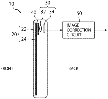
a camera located at a back side of the display, the camera including an optical lens and an imaging sensor to sense the light through the display to create an image; and
an optical element between the display and the camera, wherein the optical element filters the light through the display and passes the filtered light to the camera, and the optical element reduces a diffraction due to the wiring layer,
wherein the optical element includes an optical mask that has a mask region to shield the light from the display to the camera, wherein a masking pattern of the mask region corresponds to a wiring pattern of wires of the wiring layer, and wherein the mask region of the masking pattern satisfies at least one of:
the mask region of the masking pattern being provided for every other line of the wires of the wiring pattern;
the mask region of the masking pattern being provided for a plurality of the wires of the wiring pattern of the wiring layer;
the mask region being enlarged in areas behind around intersections of the wires; or
the mask region being formed in areas behind around the intersections of the wires and the mask region being not formed in the other areas.
|