| CPC H01L 27/1443 (2013.01) [H01L 21/0217 (2013.01); H01L 21/02274 (2013.01); H01L 21/02488 (2013.01); H01L 21/02565 (2013.01); H01L 21/02631 (2013.01); H01L 29/66969 (2013.01)] | 12 Claims |
|
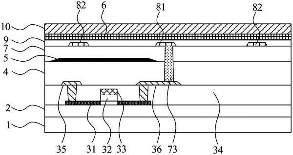
1. A photodetector, comprising a photosensitive layer, a thin film transistor, and a sensing electrode, the sensing electrode below the photosensitive layer and above the thin film transistor and connected to one of source/drain electrode of the thin film transistor to transmit a signal generated by the photosensitive layer to the thin film transistor;
wherein the photodetector further comprises a hydrogen barrier layer which is disposed between the photosensitive layer and the thin film transistor and is configured to inhibit hydrogen of the photosensitive layer from entering the thin film transistor;
wherein the photodetector further comprises a light-shielding pattern disposed between the thin film transistor and the sensing electrode and configured to block at least part of light irradiating the thin film transistor, wherein the hydrogen barrier layer is disposed above the light-shielding pattern and below the photosensitive layer.
|