US 11,894,397 B2
Semiconductor device and fabrication method of semiconductor device
Shunpei Yamazaki, Tokyo (JP); Yuichi Sato, Kanagawa (JP); and Hitoshi Nakayama, Kanagawa (JP)
Assigned to Semiconductor Energy Laboratory Co., Ltd., Kanagawa-ken (JP)
Filed by SEMICONDUCTOR ENERGY LABORATORY CO., LTD., Atsugi (JP)
Filed on Apr. 26, 2022, as Appl. No. 17/729,017.
Application 17/729,017 is a continuation of application No. 17/041,852, granted, now 11,355,530, previously published as PCT/IB2019/052744, filed on Apr. 4, 2019.
Claims priority of application No. 2018-076694 (JP), filed on Apr. 12, 2018; and application No. 2018-076752 (JP), filed on Apr. 12, 2018.
Prior Publication US 2022/0262828 A1, Aug. 18, 2022
Int. Cl. H01L 27/12 (2006.01); H01L 29/24 (2006.01); H10B 12/00 (2023.01)
CPC H01L 27/1255 (2013.01) [H01L 27/1225 (2013.01); H01L 29/24 (2013.01); H10B 12/30 (2023.02)] 8 Claims
OG exemplary drawing
 
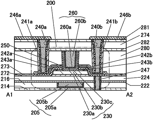
1. A semiconductor device comprising:
a first insulator;
a first conductor in an opening in the first insulator;
a first oxide over the first insulator;
a second conductor over the first oxide;
a second insulator over the second conductor;
a third conductor over the second conductor; and
a fourth conductor over the first oxide,
wherein the fourth conductor is provided in an opening in the second insulator, and
wherein the second conductor is in contact with a top surface of the first conductor and a bottom surface of the third conductor.