| CPC H01L 27/124 (2013.01) [C25D 7/123 (2013.01); C25D 17/007 (2013.01); H01L 27/127 (2013.01); H01L 27/156 (2013.01)] | 12 Claims |
|
1. A method for preparing an array substrate, comprising:
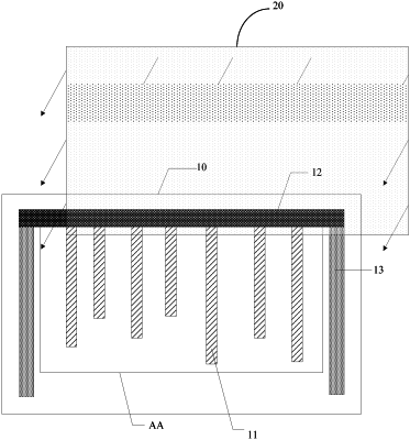
forming a pattern of a seed layer in a wiring region of a base substrate;
forming a pattern of a lead electrode at a first side of the wiring region, the lead electrode being electrically connected with the seed layer;
forming a pattern of a blocking dam on a side, where the pattern of the seed layer is formed, of the base substrate, the pattern of the seed layer being complementary with the pattern of the blocking dam; and
electroplating a pattern of a first metal layer on the pattern of the seed layer, and when electroplating the pattern of the first metal layer, connecting the lead electrode with a negative pole of a power supply;
wherein before said electroplating the pattern of the first metal layer on the pattern of the seed layer, the method further comprises:
forming a pattern of a compensation electrode wire electrically connected with the lead electrode on a side, where the lead electrode is formed, of the base substrate;
wherein the compensation electrode wire is at least at a second side of the wiring region, and the first side and the second side are different sides of the wiring region.
|