| CPC H01L 27/124 (2013.01) [H01L 27/1225 (2013.01); H01L 27/15 (2013.01); H01L 29/42384 (2013.01); H01L 29/78633 (2013.01); H10K 59/12 (2023.02)] | 20 Claims |

|
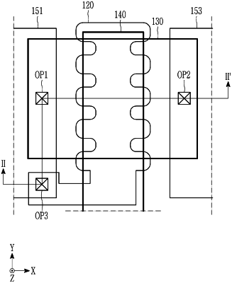
1. A display device comprising
a substrate and
a transistor on the substrate,
wherein the transistor includes:
a lower layer having conductivity and including a body portion and a plurality of protrusions;
an oxide semiconductor layer including a channel region, a first conductive region disposed at a first side of the channel region, and a second conductive region disposed at a second side of the channel region, wherein the second side is opposite the first side;
a gate electrode overlapping the channel region in a plan view;
a first electrode electrically connected to the first conductive region; and
a second electrode electrically connected to the second conductive region,
wherein the plurality of protrusions protrudes from an overlapped region where the body portion and the channel region overlap each other,
wherein the plurality of protrusions include a plurality of first protrusions extending in a first direction and a plurality of second protrusions extending in a direction opposite to the first direction.
|