| CPC H01L 27/124 (2013.01) [G02F 1/1339 (2013.01); G02F 1/13629 (2021.01); H01L 27/1288 (2013.01); H10K 59/1315 (2023.02); H10K 59/1201 (2023.02)] | 12 Claims |
|
1. A display substrate, comprising:
a base substrate;
a connection electrode on the base substrate;
a conductive sealant which is at a side, away from the base substrate, of the connection electrode and is electrically connected with the connection electrode via a plurality of via-holes respectively in different layers; and
a bridge electrode which is at least partially in at least one via-hole of the plurality of via-holes, and is electrically connected with the connection electrode and the conductive sealant,
wherein in a direction perpendicular to a surface of the base substrate on which the connection electrode is provided, the plurality of via-holes are at least partially not overlapped with each other;
the display substrate comprises:
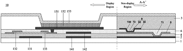
a display region comprising a plurality of pixels, wherein each of the plurality of pixels comprises a first display electrode, and a second display electrode at a side, away from the base substrate, of the first display electrode; and
a non-display region at a periphery of the display region, wherein the connection electrode, the conductive sealant and the bridge electrode are in the non-display region;
the plurality of via-holes comprise a first via-hole and a second via-hole that are respectively in different layers,
the display substrate further comprises: a first insulation layer and a second insulation layer, the first insulation layer is at the side, away from the base substrate, of the connection electrode, and the second insulation layer is at a side, away from the base substrate, of both the first insulation layer and the bridge electrode, the first via-hole penetrates through the first insulation layer and does not penetrates through the second insulation layer, and the second via-hole penetrates through the second insulation layer and does not penetrates through the first insulation layer, the first via-hole and the second via-hole are at least partially not overlapped with each other in the direction perpendicular to the surface of the base substrate;
the first via-hole exposes at least a part of the connection electrode, a part of the bridge electrode is in the first via-hole and contacts the connection electrode to be electrically connected with the connection electrode;
the second via-hole exposes at least a part of the bridge electrode, a part of the conductive sealant is in the second via-hole and is electrically connected with the connection electrode;
the conductive sealant is on a side, away from the base substrate, of the entire bridge electrode, and the entire bridge electrode is between the entire conductive sealant and the connection electrode in the direction perpendicular to the surface of the base substrate, and the conductive sealant covers the entire second via hole;
both a total number of the connection electrode and a total number of the first via-hole are at least one, and a total number of the second via-hole is multiple.
|