| CPC H01L 27/124 (2013.01) [H01L 27/127 (2013.01); H01L 27/1222 (2013.01); H01L 27/1288 (2013.01)] | 20 Claims |
|
1. A display substrate, comprising a pad bending region;
in the pad bending region, the display substrate comprising a base, and an inorganic insulating layer and a metal layer laminated on the base;
wherein the metal layer comprises a plurality of discrete metal wires, and the inorganic insulating layer comprises a plurality of discrete first inorganic insulating layers, each of which is arranged between a respective one of the plurality of discrete metal wires and the base,
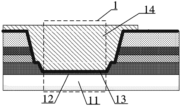
wherein in a region outside the pad bending region, the inorganic insulating layer is also present between the plurality of discrete metal wires, and an organic insulating layer is provided on the metal wires and in direct contact with the metal wires, and wherein a cross-section of metal wires along an extending direction of the metal wires and passing through the metal wires is of concave shape with two end parts extending along the extending direction of the metal wires, and a first end part of the metal wires is covered by the organic insulating layer, and a second end part of the metal wires is partially covered by the organic insulating layer, and
wherein the inorganic insulating layer is in physical contact with the metal wires and the base, and comprises a buffer layer, a first insulating layer, a second insulating layer and an interlayer insulating layer.
|