| CPC H01L 27/1225 (2013.01) [H01L 27/12 (2013.01); H01L 27/127 (2013.01); H01L 27/1288 (2013.01); H01L 29/41733 (2013.01); H01L 29/7869 (2013.01); H01L 29/78633 (2013.01)] | 20 Claims |
|
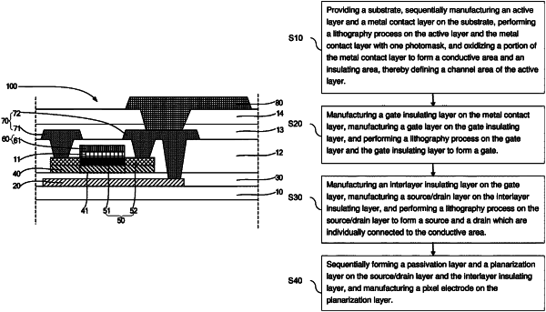
1. An array substrate, comprising:
a substrate;
an active layer disposed on the substrate and comprising a channel area;
a metal contact layer disposed on the active layer and comprising a conductive area and an insulating area, wherein the insulating area corresponds to the channel area, and the conductive area is disposed at two sides of the insulating area;
a gate insulating layer disposed on the metal contact layer;
a gate layer disposed on the gate insulating layer and comprising a gate, wherein the gate is disposed above the channel area;
a source/drain layer disposed on the conductive area and comprising a source and a drain; and
a pixel electrode disposed on the source/drain layer and connected to the source or the drain;
wherein the source and the drain are individually connected to the conductive area.
|