| CPC H01L 27/1214 (2013.01) [H01L 27/1225 (2013.01); H01L 27/156 (2013.01); H01L 29/4908 (2013.01); H01L 29/7869 (2013.01); H01L 29/78606 (2013.01); H01L 29/78696 (2013.01); H01L 33/54 (2013.01); H01L 33/62 (2013.01)] | 13 Claims |
|
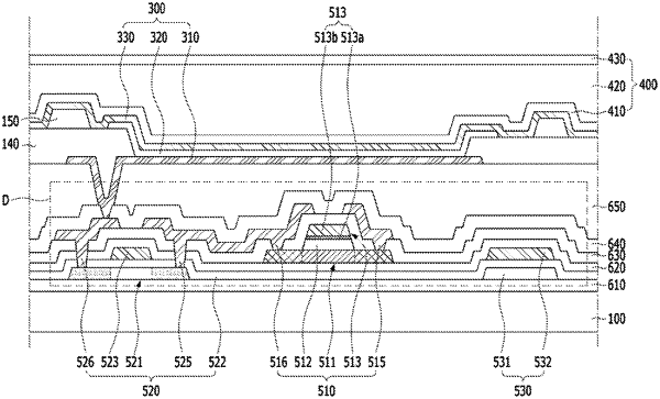
1. A display apparatus comprising:
a driving circuit on a device substrate, the driving circuit including a first thin film transistor and a second thin film transistor;
a first insulating layer on the first thin film transistor and the second thin film transistor of the driving circuit;
a second insulating layer on the first insulating layer;
a light-emitting device on the second insulating layer, the light-emitting device being electrically connected to the second thin film transistor of the driving circuit;
a bank insulating layer on the second insulating layer, the bank insulating layer includes an opening; and
a spacer on the bank insulating layer,
wherein the light-emitting device includes a first electrode, a light-emitting layer and a second electrode, which are sequentially stacked on a portion of the second insulating layer exposed by the opening of the bank insulating layer,
wherein the light-emitting layer and the second electrode extend on the bank insulating layer,
wherein an end of the light-emitting layer is spaced away from the spacer on the bank insulating layer,
wherein each of the first thin film transistor and the second thin film transistor includes an oxide semiconductor pattern and a gate electrode overlapping a portion of the oxide semiconductor pattern, and
wherein the gate electrode has a stacked structure of a first hydrogen barrier layer and a low-resistance electrode layer.
|