| CPC H01L 27/1203 (2013.01) [H01L 21/743 (2013.01); H01L 23/535 (2013.01)] | 20 Claims |
|
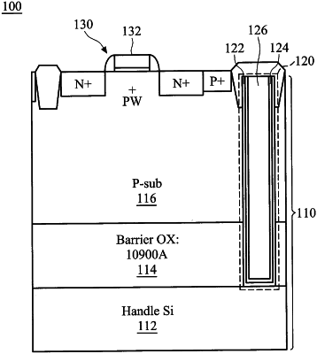
1. A silicon-on-insulator (SOI) structure, comprising:
a substrate that includes:
a handle layer,
an insulation layer comprising silicon dioxide and arranged over the handle layer,
a buried layer arranged over the insulation layer, and
a trench extending downward from an upper surface of the buried layer and terminating in the handle layer;
a dielectric layer comprising a bottom portion that extends along and is located on a bottom surface of the trench and contacting the handle layer, wherein
the dielectric layer comprises: a first sub-layer of lining oxide, and a second sub-layer of pad oxide that is formed on the first sub-layer and is thicker than the first sub-layer,
the bottom portion of the dielectric layer comprises a first bottom portion of the first sub-layer and a second bottom portion of the second sub-layer; and
a polysilicon region filling the trench, wherein a first bottom surface and a first side surface of the polysilicon region contact the second sub-layer in the dielectric layer, wherein a second bottom surface and a second side surface of the second sub-layer contact the first sub-layer, and wherein a first top surface of the polysilicon region is lower than a second top surface of the first sub-layer and a third top surface of the second sub-layer.
|