| CPC H01L 27/0924 (2013.01) [H01L 21/02192 (2013.01); H01L 21/266 (2013.01); H01L 21/823431 (2013.01); H01L 21/823437 (2013.01); H01L 21/823481 (2013.01); H01L 21/823821 (2013.01); H01L 21/823828 (2013.01); H01L 21/823878 (2013.01); H01L 21/845 (2013.01); H01L 27/0886 (2013.01); H01L 29/0642 (2013.01); H01L 29/0649 (2013.01); H01L 29/165 (2013.01); H01L 29/4966 (2013.01); H01L 29/66545 (2013.01); H01L 29/66818 (2013.01); H01L 29/7846 (2013.01); H01L 29/7854 (2013.01); H01L 29/513 (2013.01); H01L 29/517 (2013.01)] | 19 Claims |
|
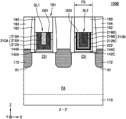
1. A method of fabricating an integrated circuit device, the method comprising:
forming an insulating structure on an active region, the insulating structure defining a plurality of gate spaces;
forming a gate stack structure in a first gate space of the plurality of gate spaces, the gate stack structure comprising a first conductive metal nitride layer and having a first effective work function; and
forming an isolation stack structure in a second gate space of the plurality of gate spaces that is adjacent the first gate space, the isolation stack structure comprising a second conductive metal nitride layer and having a second effective work function that is different than the first effective work function, the second conductive metal nitride layer comprising a same metal nitride as a metal nitride comprised in the first conductive metal nitride layer and having a different thickness than the first conductive metal nitride layer;
wherein forming the isolation stack structure comprises:
forming an interfacial layer on the active region;
forming a gate insulating layer on the interfacial layer;
forming a La-containing layer on the gate insulating layer; and
forming the second conductive metal nitride layer on the La-containing layer.
|