| CPC H01L 27/0922 (2013.01) [H01L 21/823842 (2013.01); H01L 21/823864 (2013.01); H01L 27/092 (2013.01)] | 17 Claims |
|
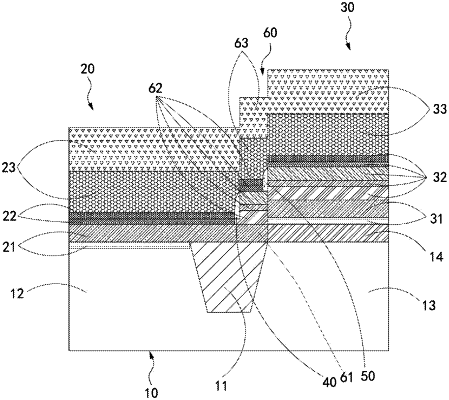
1. A semiconductor structure, comprising a substrate, and an N-channel metal-oxide semiconductor (NMOS) transistor and a P-channel metal-oxide semiconductor (PMOS) transistor that are located on the substrate, wherein
the NMOS transistor comprises:
a first dielectric layer, located on the substrate;
a first work function layer, located on the first dielectric layer; and
a first conductive layer, located on the first work function layer; and
the PMOS transistor comprises:
a second dielectric layer, located on the substrate;
a second work function layer, located on the second dielectric layer; and
a second conductive layer, located on the second work function layer;
the first work function layer is provided with a first sidewall isolation layer on a side facing the second work function layer,
the second work function layer is provided with a second sidewall isolation layer on a side facing the first work function layer; and
the first sidewall isolation layer is located below the second sidewall isolation layer.
|