| CPC H01L 27/0886 (2013.01) [H01L 21/823412 (2013.01); H01L 21/823431 (2013.01); H01L 29/7851 (2013.01)] | 20 Claims |

|
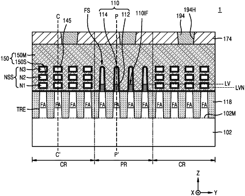
1. A method of manufacturing an integrated circuit device, the method comprising:
preparing a substrate having a cell region and a peripheral circuit region;
forming a first stacked structure on the substrate, the first stacked structure including a plurality of sacrificial semiconductor layers and a plurality of nano-sheet semiconductor layers, the plurality of sacrificial semiconductor layers and the plurality of nano-sheet semiconductor layers being alternately stacked one-by-one on the substrate;
forming a stack recess by removing a portion of the first stacked structure in the peripheral circuit region;
forming a second stacked structure on the substrate in the peripheral circuit region, the second stacked structure including a lower semiconductor layer on the substrate and an upper semiconductor layer on the lower semiconductor layer;
forming a plurality of fin-type active regions in the cell region and the peripheral circuit region defined by trenches by etching an upper portion of the substrate, a plurality of third stacked structures on the plurality of fin-type active regions in the cell region by etching the first stacked structure, and a plurality of fourth stacked structures on the plurality of fin-type active regions in the peripheral circuit region by etching the second stacked structure, the plurality of fin-type active regions extending in a first horizontal direction, each of the plurality of third stacked structures including portions of the sacrificial semiconductor layers and a plurality of nano-sheets that are portions of the plurality of nano-sheet semiconductor layers, and each of the plurality of fourth stacked structures including a portion of the lower semiconductor layer and a portion of the upper semiconductor layer;
forming a device isolation layer filling the trenches;
forming a plurality of source/drain regions on the on the plurality of fin-type active regions and the plurality of fourth stacked structures;
removing portions of the sacrificial semiconductor layers; and
forming a plurality of gate electrodes extending in a second horizontal direction crossing the first horizontal direction on the plurality of fin-type active regions,
wherein the forming the second stacked structure comprises:
forming the lower semiconductor layer on the substrate through an epitaxial growth at a first temperature by using the substrate exposed in the peripheral circuit region as the seed;
forming a semiconductor amorphous layer on the lower semiconductor layer; and
forming the upper semiconductor layer by crystallizing the semiconductor amorphous layer.
|