US 11,894,370 B2
Semiconductor structure cutting process and structures formed thereby
Ryan Chia-Jen Chen, Hsinchu (TW); Cheng-Chung Chang, Kaohsiung (TW); Shao-Hua Hsu, Taitung (TW); Yu-Hsien Lin, Kaohsiung (TW); Ming-Ching Chang, Hsinchu (TW); Li-Wei Yin, Hsinchu (TW); Tzu-Wen Pan, Hsinchu (TW); and Yi-Chun Chen, Hsinchu (TW)
Assigned to TAIWAN SEMICONDUCTOR MANUFACTURING CO., LTD., Hsinchu (TW)
Filed by Taiwan Semiconductor Manufacturing Co., Ltd., Hsinchu (TW)
Filed on Aug. 9, 2022, as Appl. No. 17/818,405.
Application 16/205,422 is a division of application No. 15/797,626, filed on Oct. 30, 2017, granted, now 10,325,912, issued on Jun. 18, 2019.
Application 17/818,405 is a continuation of application No. 16/205,422, filed on Nov. 30, 2018, granted, now 11,502,076.
Prior Publication US 2022/0384269 A1, Dec. 1, 2022
This patent is subject to a terminal disclaimer.
Int. Cl. H01L 21/76 (2006.01); H01L 29/06 (2006.01); H01L 27/088 (2006.01); H01L 27/02 (2006.01); H01L 29/66 (2006.01); H01L 21/8234 (2006.01); H01L 21/3065 (2006.01); H01L 29/78 (2006.01); H01L 21/3213 (2006.01); H01L 21/762 (2006.01); H01L 21/321 (2006.01); H01L 21/308 (2006.01); H01L 21/3105 (2006.01)
CPC H01L 27/0886 (2013.01) [H01L 21/3065 (2013.01); H01L 21/32133 (2013.01); H01L 21/76224 (2013.01); H01L 21/76229 (2013.01); H01L 21/823431 (2013.01); H01L 21/823437 (2013.01); H01L 21/823481 (2013.01); H01L 27/0207 (2013.01); H01L 29/0649 (2013.01); H01L 29/66545 (2013.01); H01L 29/7842 (2013.01); H01L 21/3086 (2013.01); H01L 21/31053 (2013.01); H01L 21/3212 (2013.01)] 20 Claims
OG exemplary drawing
 
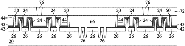
1. A structure comprising:
a first fin and a second fin protruding from a substrate;
a first isolation region over the substrate between the first fin and the second fin;
a first gate structure on the first fin;
a first insulating structure on the first isolation region; and
a second insulating structure adjacent the first insulating structure, wherein the first insulating structure is between the second insulating structure and the first gate structure, wherein the second insulating structure contacts a sidewall of the first isolation region, wherein an upper surface of the second insulating structure is level with an upper surface of the first insulating structure and an upper surface of the first gate structure.