| CPC H01L 27/0262 (2013.01) [H01L 29/7436 (2013.01)] | 8 Claims |
|
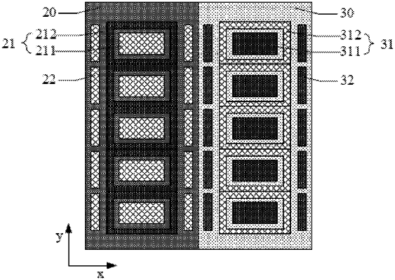
1. A semiconductor device, comprising:
a doped well region of a first conductive type;
M first semiconductor components, wherein the M first semiconductor components are provided in the doped well region of the first conductive type and are arranged in the doped well region of the first conductive type in a first direction, M being a positive integer, and wherein each first semiconductor component comprises a first doped region of a second conductive type and a first doped region of a first conductive type, and the first doped region of the first conductive type surrounds the first doped region of the second conductive type; and
second doped regions of a second conductive type, wherein the second doped regions of the second conductive type are provided on at least one side of the M first semiconductor components in the first direction, and the second doped regions of the second conductive type are spaced apart from an edge of the doped well region of the first conductive type by a fixed distance in a second direction, the first direction being perpendicular to the second direction,
wherein the second doped regions of the second conductive type are a plurality of strip-like structures spaced apart from each other in the first direction, and each of the plurality of strip-like structures is arranged corresponding to a respective one of the first semiconductor components.
|