| CPC H01L 27/0262 (2013.01) | 20 Claims |
|
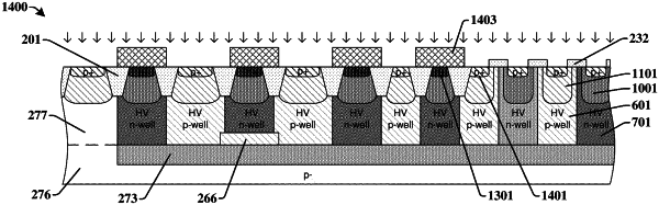
1. A method of forming an electrostatic discharge protection device on an integrated chip, the method comprising:
forming an NPN bipolar junction transistor in a semiconductor substrate, the NPN bipolar junction transistor comprising an n-doped emitter, a p-doped base, and an n-doped collector;
forming a PNP bipolar junction transistor in the semiconductor substrate, the PNP bipolar junction transistor comprising a p-doped emitter, an n-doped base, and a p-doped collector; and
forming a metal interconnect comprising:
a first metal structure that couples an anode terminal to the p-doped emitter, the n-doped base, and the n-doped emitter;
a second metal structure that couples a cathode terminal to the n-doped collector; and
a third metal structure that couples the p-doped collector to the p-doped base;
wherein the p-doped collector and the p-doped base are physically separated from one another.
|