| CPC H01L 27/0255 (2013.01) [H01L 21/823481 (2013.01); H01L 21/84 (2013.01); H01L 27/0296 (2013.01); H01L 27/1207 (2013.01); H01L 27/1211 (2013.01)] | 9 Claims |
|
1. A semiconductor device, comprising:
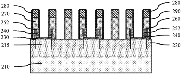
a first field effect device on a first region of a substrate, wherein a gate structure and a first source/drain of the first field effect device are separated from the substrate by a bottom dielectric layer; and
an electrostatic discharge device on a second region of the substrate, wherein a gate structure for the electrostatic discharge device is separated from the substrate by the bottom dielectric layer, and a source/drain for the electrostatic discharge device is in electrical contact with the substrate, wherein the source/drain for the electrostatic discharge device is doped with a second dopant type.
|