| CPC H01L 25/18 (2013.01) [H01L 23/481 (2013.01); H01L 23/522 (2013.01); H01L 23/5383 (2013.01); H01L 24/09 (2013.01); H01L 24/17 (2013.01); H01L 25/0652 (2013.01); H01L 25/16 (2013.01); H01L 25/50 (2013.01); H01L 23/49816 (2013.01); H01L 2924/1432 (2013.01)] | 23 Claims |
|
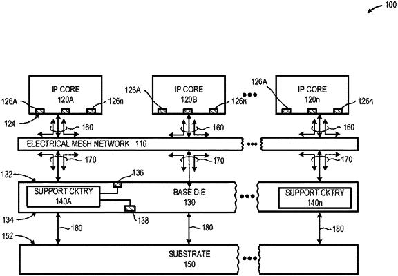
1. A method, comprising:
forming a first plurality of conductors on an upper surface of a base die;
forming a second plurality of conductors on the upper surface of the base die, wherein:
each of the first plurality of conductors is disposed on the upper surface of the base die and is spaced apart from the remaining first plurality of conductors;
each of the second plurality of conductors is disposed on the upper surface of the base die and is spaced apart from the remaining second plurality of conductors; and
each of the first plurality of conductors intersects and conductively couples to at least one of the second plurality of conductors on the upper surface of the base die, the first plurality of conductors and the second plurality of conductors conductively coupled to circuitry included in the base die; and
conductively coupling each of a plurality of cores to a node formed by an intersection of one of the first plurality of conductors with one of the second plurality of conductors, wherein each of the plurality of cores comprises processor core circuitry.
|
|
13. An apparatus, comprising:
a first plurality of conductors on an upper surface of a base semiconductor die;
a second plurality of conductors on the upper surface of the base semiconductor die, wherein:
each of the first plurality of conductors is disposed on the upper surface of the base semiconductor die and is spaced apart from the remaining first plurality of conductors;
each of the second plurality of conductors is disposed on the upper surface of the base semiconductor die and is spaced apart from the remaining second plurality of conductors; and
each of the first plurality of conductors intersects and conductively couples to at least one of the second plurality of conductors on the upper surface of the base semiconductor die, the first plurality of conductors and the second plurality of conductors conductively coupled to circuitry included in the base semiconductor die; and
each of a plurality of cores conductively coupled to a node formed by an intersection of one of the first plurality of conductors with one of the second plurality of conductors, wherein each of the plurality of cores comprises processor core circuitry.
|