| CPC H01L 25/18 (2013.01) [H01L 21/4857 (2013.01); H01L 21/561 (2013.01); H01L 21/568 (2013.01); H01L 21/78 (2013.01); H01L 23/3135 (2013.01); H01L 23/367 (2013.01); H01L 23/42 (2013.01); H01L 23/5383 (2013.01); H01L 24/16 (2013.01); H01L 24/94 (2013.01); H01L 33/54 (2013.01); H01L 33/62 (2013.01); H01L 2224/16225 (2013.01); H01L 2933/005 (2013.01)] | 10 Claims |
|
1. A system-level packaging method for a light emitting diode (LED) chip, comprising:
providing a chip wafer, comprising a first surface and a second surface opposite to each other, wherein the chip wafer comprises a plurality of first chips;
forming a plurality of connecting pillar structures on the first surface of the chip wafer to electrically lead out the first chips;
forming a first packaging layer on the first surface of the chip wafer, wherein the first packaging layer covers the connecting pillar structures;
cutting the chip wafer to form a plurality of first-chip initial packaging structures, wherein the plurality of first chips and the plurality of connecting pillar structures are arranged in respective one of the plurality of first chips, and wherein the first packaging layer covers the plurality of connecting pillar structures;
providing a supporting substrate, forming a separation layer on the supporting substrate, and attaching second surfaces of the plurality of first-chip initial packaging structures on the separation layer;
forming a second packaging layer on the separation layer, wherein the second packaging layer covers the plurality of first-chip initial packaging structures, and thinning the second packaging layer to expose the connecting pillar structures;
preparing a rewiring layer on the second packaging layer, wherein the rewiring layer is electrically connected to the plurality of connecting pillar structures;
peeling off the supporting substrate using the separation layer to expose the second surfaces of the first-chip initial packaging structures, and performing cutting to obtain first-chip intermediate packaging structures;
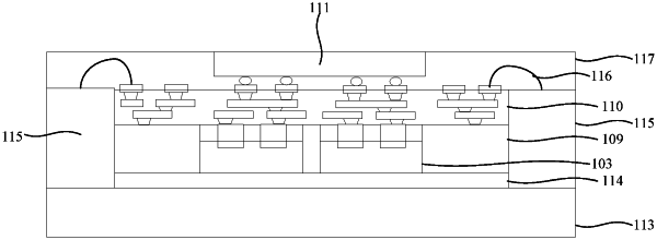
providing an LED chip and attaching the LED chip on a side of the rewiring layer away from the first-chip initial packaging structures, to obtain an integrated chip packaging structure;
forming the integrated chip packaging structure on a heat sink structure and electrically connecting the side of the rewiring layer with the LED chip formed thereon to a printed circuit board (PCB) by a metal lead wire;
forming a third packaging layer at least around the LED chip to obtain a System-in-Package (SiP) structure for an LED chip; and
forming a protective layer on the separation layer, wherein the plurality of first-chip initial packaging structures are formed on a surface of the protective layer; and
removing the protective layer after the supporting substrate is peeled off.
|