| CPC H01L 25/167 (2013.01) [H01L 27/124 (2013.01); H01L 27/1259 (2013.01)] | 15 Claims |
|
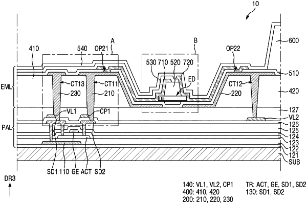
1. A display device comprising:
a first conductive layer disposed on a substrate;
a passivation layer disposed on the first conductive layer;
a second conductive layer disposed on the passivation layer;
a via layer disposed on the second conductive layer;
a third conductive layer disposed on the via layer, the third conductive layer including:
a first electrode;
a second electrode; and
a connection pattern, the first electrode, the second electrode, and the connection pattern being spaced apart from each other; and
a light emitting element, a first end and a second end of the light emitting element being disposed on the first electrode and the second electrode, respectively,
wherein the connection pattern electrically connects the first conductive layer and the second conductive layer through a first contact hole penetrating the via layer and the passivation layer.
|