| CPC H01L 25/167 (2013.01) [H01L 21/4853 (2013.01); H01L 21/4857 (2013.01); H01L 21/565 (2013.01); H01L 21/568 (2013.01); H01L 21/6835 (2013.01); H01L 23/3128 (2013.01); H01L 23/5383 (2013.01); H01L 23/5386 (2013.01); H01L 23/5389 (2013.01); H01L 24/19 (2013.01); H01L 24/20 (2013.01); H01L 2221/68372 (2013.01); H01L 2224/214 (2013.01)] | 16 Claims |

|
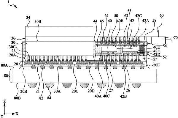
1. An optoelectronic device package, comprising:
a first redistribution layer (RDL);
a processing die; and
an input/output (I/O) die,
wherein the processing die and the I/O die are electrically connected to each other through the first RDL, the processing die comprises an active surface and an opposing surface opposite to the active surface, the I/O die includes an active surface and an opposing surface opposite to the active surface, the active surface of the processing die and the active surface of the I/O die are closer to the first RDL than the opposing surface of the processing die and the opposing surface of the I/O die; and
an electronic integrated circuit (EIC) die arranged on the first RDL, wherein the EIC die includes an active surface and an opposing surface, and the active surface of the EIC die is farther from the first RDL than the opposing surface of the EIC die,
wherein the I/O die is disposed between the processing die and the EIC die, and an edge of the first RDL protrudes out of an outer edge of the EIC die from a top view in a direction away from the I/O die.
|