US 11,894,347 B2
Low stress asymmetric dual side module
Chee Hiong Chew, Seremban (MY); Atapol Prajuckamol, Thanyaburi (TH); Stephen St. Germain, Gilbert, AZ (US); and Yusheng Lin, Phoenix, AZ (US)
Assigned to SEMICONDUCTOR COMPONENTS INDUSTRIES, LLC, Scottsdale, AZ (US)
Filed by SEMICONDUCTOR COMPONENTS INDUSTRIES, LLC, Phoenix, AZ (US)
Filed on Aug. 30, 2022, as Appl. No. 17/823,149.
Application 17/823,149 is a continuation of application No. 16/678,039, filed on Nov. 8, 2019, granted, now 11,462,515.
Claims priority of provisional application 62/882,119, filed on Aug. 2, 2019.
Prior Publication US 2022/0415857 A1, Dec. 29, 2022
This patent is subject to a terminal disclaimer.
Int. Cl. H01L 25/07 (2006.01); H01L 25/00 (2006.01); H01L 23/367 (2006.01); H01L 23/00 (2006.01)
CPC H01L 25/071 (2013.01) [H01L 23/367 (2013.01); H01L 24/32 (2013.01); H01L 25/50 (2013.01); H01L 2224/32245 (2013.01)] 20 Claims
OG exemplary drawing
 
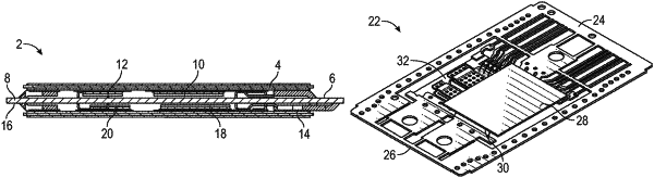
1. A semiconductor package comprising:
a first substrate;
a second substrate;
a spacer coupled between the first substrate and the second substrate;
a lead frame between the first substrate and the second substrate; and
a molding compound at least partially encapsulating the lead frame;
wherein a perimeter of the first substrate only partially overlaps a perimeter of the second substrate and the perimeter of the second substrate only partially overlaps the perimeter of the first substrate when the first substrate and second substrate are coupled through the spacer.