| CPC H01L 25/0657 (2013.01) [H01L 24/17 (2013.01); H01L 24/32 (2013.01); H01L 24/73 (2013.01); H01L 24/92 (2013.01); H01L 25/0655 (2013.01); H01L 25/105 (2013.01); H01L 25/50 (2013.01); H01L 21/563 (2013.01); H01L 23/3128 (2013.01); H01L 24/13 (2013.01); H01L 24/16 (2013.01); H01L 2224/13025 (2013.01); H01L 2224/13101 (2013.01); H01L 2224/14181 (2013.01); H01L 2224/16145 (2013.01); H01L 2224/16225 (2013.01); H01L 2224/16235 (2013.01); H01L 2224/1703 (2013.01); H01L 2224/32145 (2013.01); H01L 2224/32225 (2013.01); H01L 2224/48091 (2013.01); H01L 2224/48227 (2013.01); H01L 2224/73204 (2013.01); H01L 2224/8385 (2013.01); H01L 2224/92125 (2013.01); H01L 2225/06513 (2013.01); H01L 2225/06541 (2013.01); H01L 2225/06555 (2013.01); H01L 2225/06565 (2013.01); H01L 2225/06582 (2013.01); H01L 2225/06586 (2013.01); H01L 2225/1023 (2013.01); H01L 2225/1058 (2013.01); H01L 2924/00014 (2013.01); H01L 2924/1434 (2013.01); H01L 2924/1435 (2013.01); H01L 2924/1436 (2013.01); H01L 2924/1437 (2013.01); H01L 2924/1441 (2013.01); H01L 2924/15311 (2013.01); H01L 2924/181 (2013.01); H01L 2924/18161 (2013.01)] | 20 Claims |
|
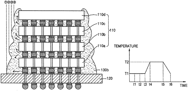
1. A semiconductor package, comprising:
a substrate base;
a first semiconductor device connected to the substrate base by a first connection terminal;
a second semiconductor device connected to the first semiconductor device by a second connection terminal;
a first underfill between the substrate base and the first semiconductor device; and
a second underfill between the first semiconductor device and the second semiconductor device,
wherein the first underfill has a first outer end in a horizontal direction parallel to an upper surface of the substrate base and the second underfill has a second outer end in the horizontal direction parallel to the upper surface of the substrate base,
a first horizontal distance from a vertical line along a side surface of the second semiconductor device to the first outer end is greater than a second horizontal distance from the side surface of the second semiconductor device to the second outer end, and
the first underfill has a first height ranging from about 5 μm to about 100 μm between the substrate base and the first semiconductor device, the second underfill has a second height of about 5 μm or greater and less than about 100 μm between the first semiconductor device and second semiconductor device, and the first height is greater than the second height.
|