US 11,894,344 B2
Power enhanced stacked chip scale package solution with integrated die attach film
Zhijun Xu, Shanghai (CN); Bin Liu, Shanghai (CN); Yong She, Shanghai (CN); and Zhicheng Ding, Shanghai (CN)
Assigned to Intel Corporation, Santa Clara, CA (US)
Filed by INTEL CORPORATION, Santa Clara, CA (US)
Filed on Apr. 6, 2022, as Appl. No. 17/714,979.
Application 17/714,979 is a continuation of application No. 16/641,221, granted, now 11,302,671, previously published as PCT/CN2017/104496, filed on Sep. 29, 2017.
Prior Publication US 2022/0230995 A1, Jul. 21, 2022
This patent is subject to a terminal disclaimer.
Int. Cl. H01L 25/065 (2023.01); H01L 23/00 (2006.01); H01L 25/18 (2023.01); H01L 25/00 (2006.01)
CPC H01L 25/0657 (2013.01) [H01L 24/73 (2013.01); H01L 24/92 (2013.01); H01L 25/18 (2013.01); H01L 25/50 (2013.01); H01L 2224/73265 (2013.01); H01L 2224/92247 (2013.01); H01L 2225/0651 (2013.01); H01L 2225/06562 (2013.01); H01L 2924/1431 (2013.01); H01L 2924/1434 (2013.01)] 19 Claims
OG exemplary drawing
 
1. An apparatus, comprising:
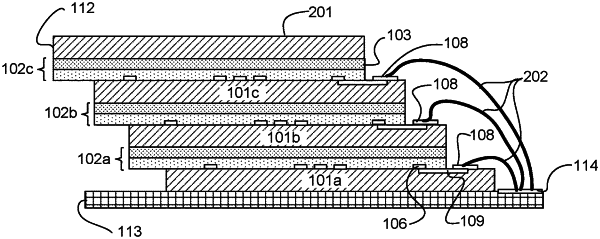
an integrated circuit (IC) die stack comprising at least a first die under a second die; and
a film between the first die and the second die, wherein the film comprises an electrically conductive layer over a first surface of the first die and an electrically insulative layer over a second surface of the second die.