| CPC H01L 25/0657 (2013.01) [H01L 23/49816 (2013.01); H01L 23/49838 (2013.01); H01L 23/5386 (2013.01); H01L 24/13 (2013.01); H01L 24/16 (2013.01); H01L 24/73 (2013.01); H01L 25/0655 (2013.01); H01L 2224/13147 (2013.01); H01L 2224/1623 (2013.01); H01L 2224/16147 (2013.01); H01L 2224/73204 (2013.01); H01L 2225/06513 (2013.01); H01L 2225/06517 (2013.01); H01L 2225/06541 (2013.01); H01L 2924/1438 (2013.01); H01L 2924/182 (2013.01); H01L 2924/1815 (2013.01)] | 17 Claims |
|
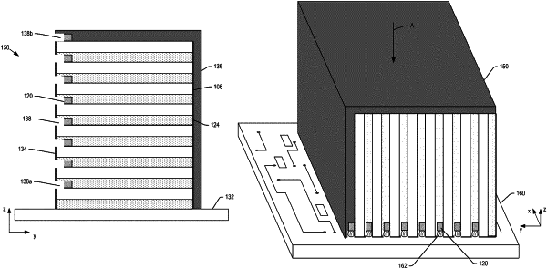
1. A semiconductor device configured to mount to a medium, the semiconductor device comprising:
a plurality of semiconductor dies, each semiconductor die comprising:
a first major surface and a second major surface,
a die attach film (DAF) on the first major surface, and
metal pillars extending from the second major surface, adjacent an edge of the semiconductor die, wherein the metal pillars on a first semiconductor die of the plurality of semiconductor dies are buried in the DAF of a second semiconductor die of the plurality of semiconductor dies next adjacent the first semiconductor die;
the plurality of semiconductor dies configured to surface mount to the medium with the edge of each semiconductor die facing the medium, the metal pillars configured to couple with electrical contacts on the medium.
|