| CPC H01L 25/0652 (2013.01) [H01L 21/4853 (2013.01); H01L 21/4857 (2013.01); H01L 21/565 (2013.01); H01L 23/3128 (2013.01); H01L 23/5383 (2013.01); H01L 23/5386 (2013.01); H01L 25/50 (2013.01); H01L 2225/06513 (2013.01); H01L 2225/06541 (2013.01); H01L 2225/06586 (2013.01)] | 20 Claims |
|
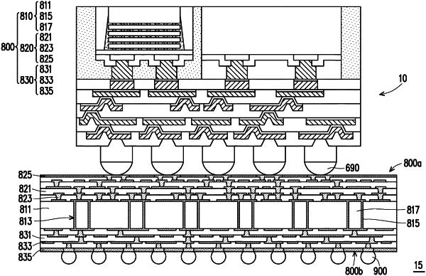
1. A semiconductor package, comprising:
a semiconductor die, comprising a contact post;
an encapsulant, encapsulating the semiconductor die;
a first dielectric layer, extending on the encapsulant and the semiconductor die;
a through via, extending through the first dielectric layer and having one end contacting the contact post of the semiconductor die;
an extension pad disposed on the first dielectric layer and contacting an opposite end of the through via with respect to the contact post, wherein the extension pad has an elongated shape, a first end of the extension pad overlaps with the contact post and the through via, and a second end of the extension pad overlaps with the encapsulant;
a second dielectric layer, disposed on the first dielectric layer and the extension pad; and
a routing via, extending through the second dielectric layer to contact the second end of the extension pad.
|