| CPC H01L 25/0652 (2013.01) [H01L 21/78 (2013.01); H01L 23/16 (2013.01); H01L 23/3128 (2013.01); H01L 23/49822 (2013.01); H01L 23/562 (2013.01); H01L 25/50 (2013.01)] | 10 Claims |
|
1. A package structure, comprising:
a wiring structure including at least one dielectric layer, and at least one circuit layer in contact with the dielectric layer;
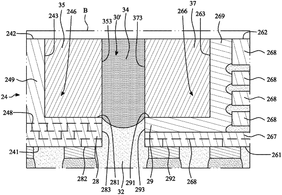
a first electronic device electrically connected to the wiring structure, and the first electronic device having a first surface, a second surface and at least one lateral side surface extending between the first surface and the second surface, wherein the first electronic device includes a first active circuit region and a first protrusion portion, the first protrusion portion protrudes from the at least one lateral side surface of the first electronic device, and a portion of the first active circuit region is disposed in the first protrusion portion, wherein the first protrusion portion of the first electronic device has an upper surface, a lower surface and an outer side surface extending between the upper surface and the lower surface, and the upper surface of the first protrusion portion and the at least one lateral side surface of the first electronic device define an indentation structure; and
a first underfill-repelling material disposed in the indentation structure.
|