US 11,894,338 B2
Wafer level package
Jinwoo Park, Hwaseong-si (KR); Jungho Park, Cheonan-si (KR); Dahye Kim, Gwangmyeong-si (KR); and Minjun Bae, Yongin-si (KR)
Assigned to Samsung Electronics Co., Ltd., Gyeongg-do (KR)
Filed by Samsung Electronics Co., Ltd., Suwon-si (KR)
Filed on Feb. 4, 2022, as Appl. No. 17/592,947.
Application 17/592,947 is a continuation of application No. 16/869,988, filed on May 8, 2020, granted, now 11,264,354.
Claims priority of application No. 10-2019-0124772 (KR), filed on Oct. 8, 2019.
Prior Publication US 2022/0157772 A1, May 19, 2022
This patent is subject to a terminal disclaimer.
Int. Cl. H01L 23/00 (2006.01); H01L 25/065 (2023.01); H01L 23/31 (2006.01)
CPC H01L 24/94 (2013.01) [H01L 23/3121 (2013.01); H01L 24/14 (2013.01); H01L 25/0657 (2013.01)] 18 Claims
OG exemplary drawing
 
1. A package comprising:
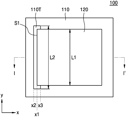
a semiconductor chip on a package substrate, the package substrate including a trench having a line shape, the trench extending in a first direction along a first side surface of the semiconductor chip on the package substrate; and
an underfill filling a space between the package substrate and the semiconductor chip, the underfill filling the trench,
wherein the trench is disposed on a portion of the package substrate to overlap with at least a portion of the semiconductor chip in a second direction perpendicular to the first direction.