| CPC H01L 24/20 (2013.01) [H01L 21/4853 (2013.01); H01L 21/4857 (2013.01); H01L 23/3128 (2013.01); H01L 23/5383 (2013.01); H01L 23/5386 (2013.01); H01L 23/5389 (2013.01); H01L 24/19 (2013.01); H01L 25/105 (2013.01); H01L 2224/214 (2013.01); H01L 2224/2105 (2013.01); H01L 2225/1035 (2013.01); H01L 2225/1041 (2013.01); H01L 2225/1058 (2013.01); H01L 2924/3512 (2013.01)] | 20 Claims |
|
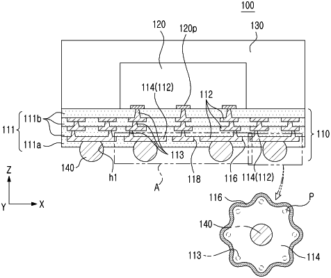
1. A semiconductor package comprising:
a redistribution substrate including a connection via and a redistribution layer electrically connected to each other, and a redistribution pad electrically connected to the redistribution layer by the connection via; and
a semiconductor chip disposed on the redistribution substrate and including a connection pad electrically connected to the redistribution layer,
wherein the redistribution pad has a shape having a plurality of protrusions protruding in directions different to each other in a plan view, and
wherein the redistribution substrate further includes a dummy metal pattern disposed between adjacent redistribution pads.
|