| CPC H01L 24/13 (2013.01) [H01L 24/05 (2013.01); H01L 24/11 (2013.01); H01L 24/16 (2013.01); H01L 2224/022 (2013.01); H01L 2224/0401 (2013.01); H01L 2224/11831 (2013.01); H01L 2224/13018 (2013.01); H01L 2224/13084 (2013.01); H01L 2224/16227 (2013.01)] | 20 Claims |
|
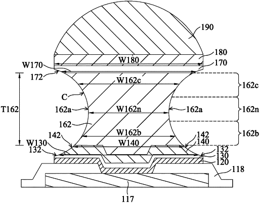
1. A chip structure, comprising:
a substrate;
an interconnect layer over the substrate;
a conductive pad over the interconnect layer;
a conductive bump over the conductive pad, wherein the conductive bump has a first portion, a second portion, and a neck portion between the first portion and the second portion, the first portion is between the neck portion and the conductive pad, and the neck portion is narrower than the first portion and narrower than the second portion; and
an alloy layer between the conductive bump and the conductive pad, wherein a first composition of the alloy layer is different from a second composition of the conductive bump, and the alloy layer has a first width decreasing toward the conductive bump.
|