| CPC H01L 24/05 (2013.01) [H01L 21/7682 (2013.01); H01L 21/76885 (2013.01); H01L 23/5226 (2013.01); H01L 23/53295 (2013.01); H01L 24/03 (2013.01); H01L 24/13 (2013.01); H01L 29/41725 (2013.01); H01L 29/4236 (2013.01); H01L 2224/0217 (2013.01); H01L 2224/0219 (2013.01); H01L 2224/02181 (2013.01); H01L 2224/02185 (2013.01); H01L 2224/02206 (2013.01); H01L 2224/02215 (2013.01); H01L 2224/03019 (2013.01); H01L 2224/0391 (2013.01); H01L 2224/0401 (2013.01); H01L 2224/05007 (2013.01); H01L 2224/05573 (2013.01); H01L 2224/10135 (2013.01)] | 12 Claims |
|
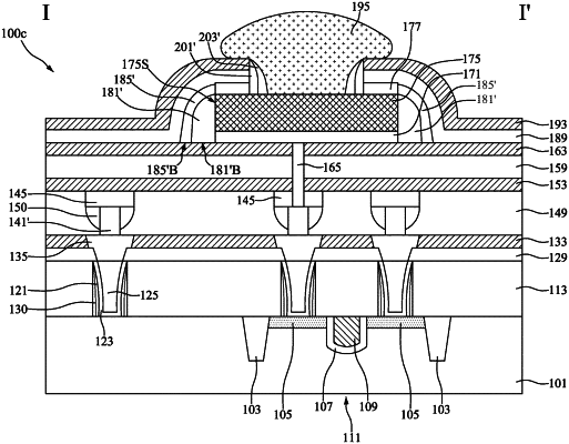
1. A semiconductor device, comprising:
a bonding pad disposed over a semiconductor substrate;
a first spacer disposed over a top surface of the bonding pad;
a dielectric liner disposed between the first spacer and the bonding pad;
a dielectric layer between the bonding pad and the semiconductor substrate, wherein the dielectric layer includes silicon-rich oxide;
a conductive bump disposed over the bonding pad and covering the first spacer and the dielectric liner, wherein the conductive bump is electrically connected to a source/drain (S/D) region in the semiconductor substrate through the bonding pad;
a second spacer disposed over a sidewall of the bonding pad and conformally covering the first spacer;
a first passivation layer covering the second spacer, wherein the first spacer is in direct contact with the first passivation layer; and
a second passivation layer between the first passivation layer and the bonding pad, wherein the second spacer is covered by the second passivation layer, and a portion of the conductive bump is surrounded by the first passivation layer and the second passivation layer.
|