| CPC H01L 23/66 (2013.01) [H01L 21/4857 (2013.01); H01L 23/5383 (2013.01); H01L 23/5386 (2013.01); H01L 24/16 (2013.01); H01L 25/0652 (2013.01); H01L 25/0655 (2013.01); H01L 25/50 (2013.01); H01L 24/17 (2013.01); H01L 2223/6627 (2013.01); H01L 2224/16146 (2013.01); H01L 2224/16227 (2013.01); H01L 2224/16238 (2013.01); H01L 2224/1703 (2013.01); H01L 2224/17181 (2013.01); H01L 2225/06513 (2013.01); H01L 2225/06517 (2013.01); H01L 2225/06541 (2013.01); H01L 2225/06568 (2013.01); H01L 2924/19033 (2013.01)] | 25 Claims |
|
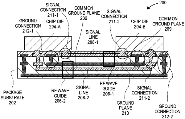
1. An electronic package comprising:
a package substrate;
a first silicon die or tile and a second silicon die or tile attached to the package substrate;
a first waveguide formed in the package substrate, the first waveguide interconnecting the first silicon die or tile with the second silicon die or tile;
a second waveguide formed in the package substrate, the second waveguide interconnecting the first silicon die or tile with the second silicon die or tile, wherein the second waveguide is vertically beneath the first waveguide; and
a conductive interconnect in the package substrate, the conductive interconnect interconnecting the first silicon die or tile with the second silicon die or tile.
|