| CPC H01L 23/552 (2013.01) [H01L 21/4846 (2013.01); H01L 21/56 (2013.01); H01L 23/49838 (2013.01); H01L 25/0655 (2013.01); H01L 23/49827 (2013.01)] | 6 Claims |
|
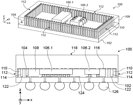
1. An electronic system in package, including at least:
a support;
one or more chips mechanically and electrically coupled to a front face of the support;
electrical contact elements disposed at a rear face, opposite to the front face, of the support, and electrically coupled to the one or more chips;
an encapsulation material covering the front face of the support and encapsulating the chip(s), and/or a cover forming, at least with the support, at least one cavity in which the chip(s) are disposed; and
several side protection elements, laterally surrounding the chip(s) and configured to form a barrier at least against laser attacks made through side faces of the electronic system in package which are substantially perpendicular to the front face of the support;
wherein the side protection elements are disposed in the encapsulation material or in one or more first blocks of material distinct from the support and disposed in the encapsulation material and/or between the support and the cover;
wherein the side protection elements comprise at least one opaque material such that a laser beam whose wavelength is between 360 nm and 1064 nm cannot pass therethrough;
wherein the side protection elements include at least one electrically conductive material; and
wherein the electronic system in package further includes at least one front protection layer of the electronic system in package, disposed in the encapsulation material, on the side of a front face of the electronic system in package and facing the chip(s), and comprising several portions of electrically conductive material extending in at least one plane parallel to the front face of the electronic system in package in at least one coil pattern.
|