US 11,894,314 B2
Semiconductor device and method of forming semiconductor package with RF antenna interposer having high dielectric encapsulation
HunTeak Lee, Gyeongi-do (KR); Gwang Kim, Gyeongi-do (KR); Junho Ye, Seoul (KR); YouJoung Choi, Gyeonggi-do (KR); MinKyung Kim, Incheon (KR); Yongwoo Lee, Incheon (KR); and Namgu Kim, Incheon (KR)
Assigned to STATS ChipPAC Pte. Ltd., Singapore (SG)
Filed by STATS ChipPAC Pte. Ltd., Singapore (SG)
Filed on Sep. 10, 2021, as Appl. No. 17/447,336.
Prior Publication US 2023/0081706 A1, Mar. 16, 2023
Int. Cl. H01L 23/52 (2006.01); H01L 23/552 (2006.01); H01L 23/31 (2006.01); H01Q 1/40 (2006.01); H01L 23/498 (2006.01); H01L 21/56 (2006.01)
CPC H01L 23/552 (2013.01) [H01L 21/56 (2013.01); H01L 23/3128 (2013.01); H01L 23/49822 (2013.01); H01Q 1/40 (2013.01)] 25 Claims
OG exemplary drawing
 
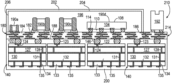
1. A method of making a semiconductor device, comprising:
providing a substrate;
disposing an electrical component over a surface of the substrate;
disposing an antenna interposer over the substrate; and
depositing a first encapsulant around the antenna interposer, wherein the first encapsulant comprises a high dielectric constant in the range of 14 to 21.