| CPC H01L 23/5389 (2013.01) [H01L 21/4853 (2013.01); H01L 21/4857 (2013.01); H01L 21/565 (2013.01); H01L 21/568 (2013.01); H01L 21/6835 (2013.01); H01L 23/3128 (2013.01); H01L 23/5383 (2013.01); H01L 23/5386 (2013.01); H01L 24/19 (2013.01); H01L 24/20 (2013.01); H01L 2221/68372 (2013.01); H01L 2224/214 (2013.01); H01L 2924/1431 (2013.01); H01L 2924/1434 (2013.01); H01L 2924/19106 (2013.01)] | 20 Claims |
|
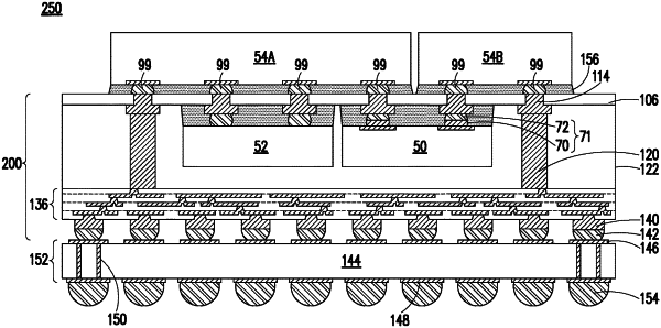
1. A method comprising:
forming a seed layer over a carrier substrate;
forming a patterned dielectric layer over the seed layer, the patterned dielectric layer comprising a plurality of openings;
plating a first metallization pattern in the plurality of openings;
bonding an interconnect device to a first surface of the first metallization pattern, the interconnect device is free of any transistors;
bonding a passive device to the first surface of the first metallization pattern, the passive device is free of any active devices;
burying the interconnect device and the passive device in a dielectric film;
bonding a first device die to a second surface of the first metallization pattern, the second surface is opposite the first surface; and
bonding a second device die to the second surface of the first metallization pattern, wherein the interconnect device electrically routes signals between the first device die and the second device die.
|