| CPC H01L 23/5389 (2013.01) [H01L 21/56 (2013.01); H01L 21/6835 (2013.01); H01L 23/3128 (2013.01); H01L 24/19 (2013.01); H01L 24/25 (2013.01); H01L 24/82 (2013.01); H01L 25/0652 (2013.01); H01L 25/0655 (2013.01); H01L 25/071 (2013.01); H01L 25/112 (2013.01); H01L 2221/68359 (2013.01); H01L 2221/68372 (2013.01); H01L 2224/0401 (2013.01); H01L 2224/16235 (2013.01); H01L 2224/16238 (2013.01); H01L 2224/22 (2013.01); H01L 2224/224 (2013.01); H01L 2224/24226 (2013.01); H01L 2224/73103 (2013.01); H01L 2224/73104 (2013.01); H01L 2224/73203 (2013.01); H01L 2224/73204 (2013.01); H01L 2224/73209 (2013.01); H01L 2224/73217 (2013.01); H01L 2224/73267 (2013.01); H01L 2924/15311 (2013.01)] | 19 Claims |
|
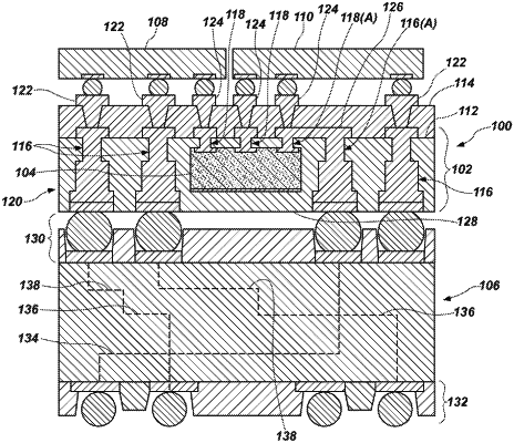
1. A microelectronic device, comprising:
an embedded die in a dielectric body, the embedded die having a first side and a second side opposite the first side;
a first vertical contact and a second vertical contact extending through the dielectric body, the first vertical contact and the second vertical contact laterally adjacent to the first side of the embedded die;
a third vertical contact and a fourth vertical contact extending through the dielectric body, the third vertical contact and the fourth vertical contact laterally adjacent to the second side of the embedded die;
a first die electrically coupled to the embedded die, and the first die electrically coupled to and vertically overlapping the first vertical contact and the second vertical contact;
a second die electrically coupled to the embedded die, the second die electrically coupled to and vertically overlapping the third vertical contact and the fourth vertical contact, wherein there is no intervening die between the second die and the first die;
an insulative layer comprising interconnects, the insulative layer over the embedded die, over the first vertical contact, over the second vertical contact, over the third vertical contact, and over the fourth vertical contact;
first contact pads above a top surface of the insulative layer, the first contact pads coupled to the first die; and
second contact pads above the top surface of the insulative layer, the second contact pads coupled to the second die.
|