| CPC H01L 23/5389 (2013.01) [H01L 21/4853 (2013.01); H01L 21/4857 (2013.01); H01L 21/565 (2013.01); H01L 21/568 (2013.01); H01L 21/6835 (2013.01); H01L 23/3128 (2013.01); H01L 23/367 (2013.01); H01L 23/5383 (2013.01); H01L 23/5386 (2013.01); H01L 23/552 (2013.01); H01L 24/19 (2013.01); H01L 24/20 (2013.01); H01L 2221/68372 (2013.01); H01L 2224/214 (2013.01); H01L 2924/3025 (2013.01)] | 16 Claims |
|
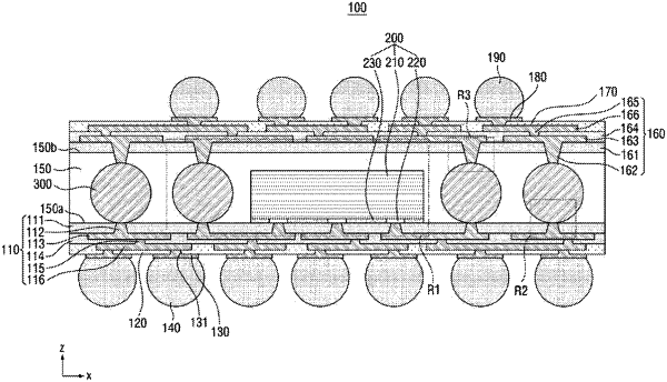
1. A fan-out semiconductor package, comprising:
a first redistribution layer;
a first semiconductor chip on the first redistribution layer;
an interconnector on the first redistribution layer and spaced apart from the first semiconductor chip;
a molded layer covering the interconnector and side surfaces of the first semiconductor chip; and
a second redistribution layer on the molded layer,
wherein:
the interconnector includes a metal ball that has a full spherical shape and is electrically connected to the first redistribution layer,
the second redistribution layer includes a first line wiring, and a first via electrically connected to the first line wiring,
the first via is connected to the interconnector,
a part of the first via is in the molded layer,
the first redistribution layer includes an insulating layer, a second line wiring, and a second via that penetrates the insulating layer and is electrically connected to the second line wiring,
the second via is connected to the interconnector,
an interface between the first via and the interconnector is a curved surface such that the first via has a rounded concavity that is complementary to the full spherical shape of the interconnector, and
an interface between the second via and the interconnector is a curved surface such that the second via has a rounded concavity that is complementary to the full spherical shape of the interconnector.
|