| CPC H01L 23/5389 (2013.01) [H01L 21/4853 (2013.01); H01L 21/4857 (2013.01); H01L 21/4871 (2013.01); H01L 21/565 (2013.01); H01L 21/78 (2013.01); H01L 22/12 (2013.01); H01L 23/3128 (2013.01); H01L 23/3675 (2013.01); H01L 23/5383 (2013.01); H01L 23/5386 (2013.01); H01L 24/19 (2013.01); H01L 24/20 (2013.01); H01L 25/105 (2013.01); H01L 2224/214 (2013.01); H01L 2225/1035 (2013.01); H01L 2225/1058 (2013.01); H01L 2924/19103 (2013.01)] | 20 Claims |
|
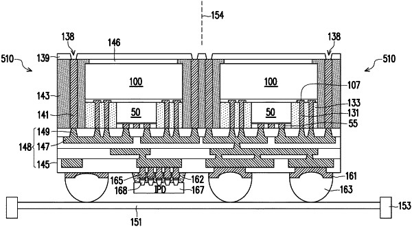
1. A semiconductor structure comprising:
a first die having a bonding pad at a first side of the first die;
a second die having a first side that faces away from the first die and having a second side attached to the first side of the first die, the second die having a die connector at the first side of the second die;
a first conductive pillar attached to the bonding pad of the first die and adjacent to the second die;
a dielectric material on the first side of the first die around the second die and around the first conductive pillar, wherein a first width of the dielectric material, measured between opposing sidewalls of the dielectric material laterally distal from the second die, is substantially the same as a second width measured between opposing sidewalls of the first die, wherein the first conductive pillar extends through the dielectric material;
a molding material around the first die, the second die, the first conductive pillar, and the dielectric material, wherein the molding material extends along and contacts the opposing sidewalls of the dielectric material and the opposing sidewalls of the first die;
a second conductive pillar in the molding material and extending through the molding material; and
a redistribution structure on the molding material and electrically coupled to the first die, the second die, the first conductive pillar, and the second conductive pillar, wherein the second die is between the first die and the redistribution structure.
|