| CPC H01L 23/5386 (2013.01) [H01L 25/075 (2013.01); H01L 33/62 (2013.01)] | 20 Claims |
|
1. A semiconductor device package comprising:
a substrate;
a plurality of semiconductor structures disposed to be spaced apart from each other at a central portion of the substrate,
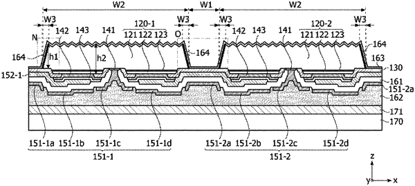
wherein the semiconductor structure is disposed on the substrate and includes a first conductivity-type semiconductor layer, a second conductivity-type semiconductor layer, and an active layer disposed between the first conductivity-type semiconductor layer and the second conductivity-type semiconductor layer,
the second conductivity-type semiconductor layer and the active layer are disposed between the first conductivity type semiconductor layer and the substrate, and
a length ratio of a maximum height of an outermost surface of the first conductivity-type semiconductor layer to a separation distance between the adjacent semiconductor structures is in a range of 1:3 to 1:60;
an intermediate layer disposed on the outermost surface of the first conductivity-type semiconductor layer,
wherein the intermediate layer overlaps the outermost surface of the first conductivity-type semiconductor layer in a direction perpendicular to a thickness direction thereof, and
the intermediate layer includes a plurality of layers and is made of any one selected from among metal, ceramic, and semiconductor materials.
|