| CPC H01L 23/5286 (2013.01) [H01L 21/8221 (2013.01); H01L 21/823475 (2013.01); H01L 21/823871 (2013.01); H01L 23/50 (2013.01); H01L 27/092 (2013.01); H10B 41/20 (2023.02); H10B 51/20 (2023.02)] | 20 Claims |
|
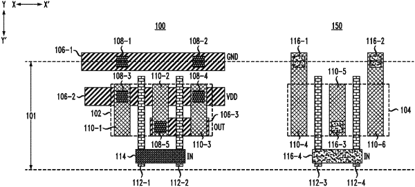
1. A method of forming a semiconductor structure comprising:
forming first and second field-effect transistors of a first type at a first vertical level of the semiconductor structure;
forming third and fourth field-effect transistors of a second type at a second vertical level of the semiconductor structure over the first vertical level of the semiconductor structure;
forming a first gate structure shared between the first and second field-effect transistors at the first vertical level;
forming a second gate structure shared between the third and fourth field-effect transistors at the second vertical level; and
forming a gate contact shared by the first and second gate structures;
wherein the first, second, third and fourth field-effect transistors provide a three-dimensional stacked transistor structure; and
wherein the first and second gate structures are vertically aligned with another in a layout of the three-dimensional stacked transistor structure between source drain/regions of the first, second, third and fourth field-effect transistors.
|