| CPC H01L 23/5283 (2013.01) [H01L 21/76805 (2013.01); H01L 21/76816 (2013.01); H01L 21/76877 (2013.01); H01L 21/76895 (2013.01); H01L 23/5226 (2013.01); H01L 23/535 (2013.01); H10B 41/10 (2023.02); H10B 41/27 (2023.02); H10B 43/10 (2023.02); H10B 43/27 (2023.02)] | 18 Claims |
|
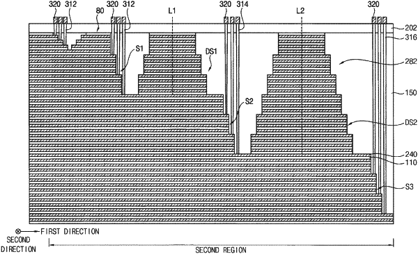
1. A vertical memory device comprising:
a substrate comprising a first region and a second region adjacent the first region;
a cell stacked structure on the first region, the cell stacked structure comprising insulation layers and gate patterns repeatedly and alternately stacked, and the gate patterns extending in a first direction;
a wiring connection structure on the second regions, the wiring connection structure contacting a first sidewall of the cell stacked structure; and
a first insulating interlayer on the substrate to cover the wiring connection structure,
wherein the wiring connection structure comprises:
a first staircase structure having one side of a stepped shape;
a second staircase structure having one side of a stepped shape and disposed below the first staircase structure; and
a first dummy staircase structure between the first and second staircase structures,
wherein the first and second staircase structures are spaced apart from each other in the first direction, and both sides in a first direction of the first dummy staircase structure have stepped shapes,
wherein an uppermost surface of the first dummy staircase structure is coplanar with an uppermost surface of the first staircase structure.
|