| CPC H01L 23/528 (2013.01) [H01L 24/80 (2013.01); H01L 29/41766 (2013.01); H10B 43/27 (2023.02); H01L 2224/80895 (2013.01)] | 20 Claims |
|
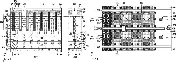
1. A semiconductor memory device, comprising:
a source structure;
a stacked conductive layer overlapping with the source structure;
a first select conductive layer and a second select conductive layer disposed between the source structure and the stacked conductive layer;
a stacked insulating layer disposed between the first select conductive layer and the stacked conductive layer and between the second select conductive layer and the stacked conductive layer;
a first slit structure and a second slit structure passing through the stacked conductive layer and the stacked insulating layer; and
a separation insulating structure passing through the source structure,
wherein the first and second slit structures and the separation insulating structure are disposed between the first select conductive layer and the second select conductive layer, and
wherein the separation insulating structure is disposed between the first slit structure and the second slit structure.
|