| CPC H01L 23/525 (2013.01) [H01L 21/56 (2013.01); H01L 23/293 (2013.01); H01L 23/3192 (2013.01); H01L 23/5225 (2013.01); H01L 23/5329 (2013.01); H01L 23/552 (2013.01); H01L 24/03 (2013.01); H01L 24/05 (2013.01); H01L 24/06 (2013.01); H01L 24/11 (2013.01); H01L 24/14 (2013.01); H01L 21/76807 (2013.01); H01L 21/76816 (2013.01); H01L 21/76885 (2013.01); H01L 23/5286 (2013.01); H01L 24/13 (2013.01); H01L 2224/0348 (2013.01); H01L 2224/03462 (2013.01); H01L 2224/0401 (2013.01); H01L 2224/05008 (2013.01); H01L 2224/05009 (2013.01); H01L 2224/05022 (2013.01); H01L 2224/05139 (2013.01); H01L 2224/05144 (2013.01); H01L 2224/05147 (2013.01); H01L 2224/05548 (2013.01); H01L 2224/05569 (2013.01); H01L 2224/05572 (2013.01); H01L 2224/11622 (2013.01); H01L 2224/13022 (2013.01); H01L 2224/13023 (2013.01); H01L 2224/13024 (2013.01); H01L 2224/16104 (2013.01)] | 20 Claims |
|
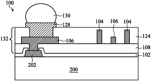
1. A method for forming a semiconductor device comprising:
forming a first insulating layer over a substrate, wherein the first insulating layer is a photosensitive material;
exposing a first portion and a second portion of the first insulating layer in a first exposure process;
exposing a third portion of the first insulating layer in a second exposure process, wherein the third portion does not overlap the first portion and the second portion;
after exposing the first portion, the second portion, and the third portion, removing the first portion, the second portion, and the third portion to form a first recess, a second recess, and a third recess, respectively, wherein the third recess has a different depth than the first recess and the second recess;
forming a conductive material in the first recess, the second recess, and the third recess to form a first conductive line in the first recess, a second conductive line in the second recess, and a third conductive line in the third recess; and
depositing a second insulating layer over the first insulating layer.
|