| CPC H01L 23/5226 (2013.01) [H01L 23/53223 (2013.01); H10B 41/10 (2023.02); H10B 41/27 (2023.02); H10B 41/35 (2023.02); H10B 43/10 (2023.02); H10B 43/27 (2023.02); H10B 43/35 (2023.02)] | 20 Claims |
|
1. A method of forming a semiconductor structure, comprising:
forming an alternating stack of insulating layers and sacrificial material layers over a substrate;
forming memory openings vertically extending through the alternating stack;
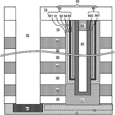
forming memory opening fill structures in the memory openings, wherein each of the memory opening fill structures comprises a memory film and a vertical semiconductor channel that extend vertically, and each memory film comprises a blocking dielectric metal oxide layer and a continuous silicon oxide liner that laterally surrounds the blocking dielectric metal oxide layer;
forming backside recesses by removing the sacrificial material layers selective to the insulating layers and the memory opening fill structures;
dividing each continuous silicon oxide liner into a respective vertical stack of silicon oxide liners by performing an etch process to physically expose segments of outer sidewalls of the respective blocking dielectric metal oxide layer;
forming a dielectric metal oxide layer directly on physically exposed surfaces of the insulating layers and directly on the physically exposed segments of the outer sidewalls of the blocking dielectric metal oxide layers; and
forming electrically conductive layers in remaining volumes of the backside recesses directly on the dielectric metal oxide layer.
|